
 |
 |
|
|
Push to Toggle
Push-button toggle function
Toggle functions are all around us in electronics. It is one of the basic
functions to perform user-interfacing. However, the digital world and simple
logic is not very forgiving when you put in a simple switch. Mechanical
switches have a nasty habit of contact bouncing. The contacts of a
mechanical switch will not touch or release immediately and a signal will
exhibit jitter for 1..10ms. This can be fatal for digital interfacing because
logic gates react very much faster (at 5 orders of magnitude). Even micro
controllers can detect bouncing switches as they are still 2..4 orders of
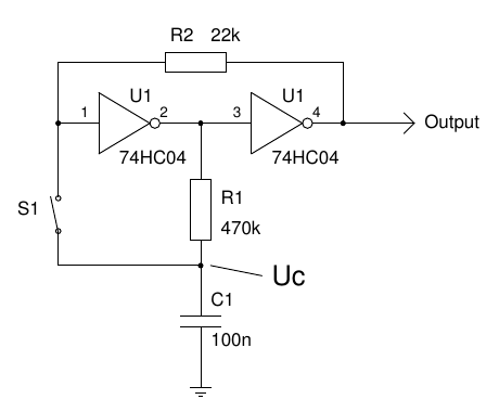
magnitude faster than the switch bouncing.On a micro controller you can easily program a push-button interface to perform both debouncing and implement a toggle function. But what about doing this in hardware? Especially, doing it with few readily available components? I recently came across a simple diagram from a mixer-table that had the toggle function implemented when I was asked to explain how it worked. The mixer-table is pre-microprocessor era and performs all functions in discrete logic. I have to admit, the elegance of the circuit is fantastic. It is a brilliant example of pre-microprocessor era ingenuity.  The above circuit is a stripped down version of the original which should illustrate the functioning (the original used NOR gates from the 4000 series). The important features of the circuit are:
 The two inverters are setup in a high-gain loop. This means a stable output in whichever state it currently is in. The switch-timing diagram below illustrates what happens when you push the button (timing not entirely to scale).  The first contact closing of the push-button causes the energy stored in the capacitor to be used to initiate the change of state. The new state will be held into place by the voltage divider R1/R2 for as long as the button is pressed. The residual jitter seen at Uc, caused by contact bouncing, is caught by the slow RC-time of R1*C1. Momentary releases of the contacts cause C1 to be reversed in charge, but that takes a long time with respect to the bounce timing. Also, every bounce of the contacts has both an on and off period, where the on-period will move C1's charge into the stable region and the off-period exhibits the R1*C1 (dis-)charge curve. The voltage at Uc with the push-button pressed is determined by the voltage divider R1 and R2. When the output turns high, then R1/R2 result in a holding voltage at 5V*470k/(470k+22k)=4.78V (assuming 5V power supply). When the output turns low, then the holding voltage at Uc will be reversed and level at 5V*22k/(470k+22k)=0.22V. When the output is high, then the capacitor C1 lacks any energy (is at 0V). In this state, the capacitor ensures a low-input at the first inverter as to initiate the change of state by requiring a long time to charge. In this state, the R1/R2 voltage divider will ensure that the capacitor will not be charged over 0.22V for as long as the button is pressed. The criteria for this circuit to work properly are in the component's relative dimensions and are rather uncritical. As a rule of thumb, the following values will work properly.
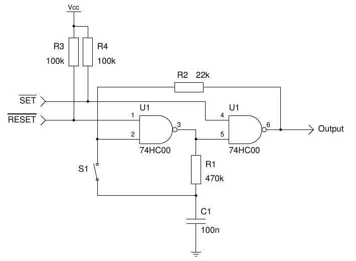
The RC-time constant should be more than the bounce-time. Most switches are guaranteed to be stable after at most 10ms. A bit of margin is appreciated and should be somewhere between a factor 2..5. A higher RC-time reduces the ability to toggle the output fast. A human can push a button (rule of thumb) at a rate of 5 times per second. An RC network is considered to be stable after 5 RC-times. Therefore the RC-time should not significantly exceed 1/5 * 1/5Hz or 40ms. A mentioned earlier, the original design used NOR gates. It also used a 4066 (analogue switch) for S1 to ensure that the actual mechanical switch was not signal referenced, but power supply referenced (contact enabled Vcc to propagate). You can, in principle, use any inverting type of gate. Using simple inverters has a disadvantage. When you turn on power, it is not guaranteed in which state the system will start. It may be either high or low. There is a very small bias towards starting with a high output, caused by the R1*C1 load, but that is no guarantee for consistency because the output impedance of the inverter is 4..5 orders of magnitude lower than the load. When you use a NOR or NAND gate, then you have the ability to set/reset the initial state of the system:  If you have multiple of these circuits, as with the mixer-table, you have the ability to use the set/reset lines to do "master-on" or "master-off" things. Something that is a nice feature to have on a mixer-table. A simple low pulse on either set or reset line will set/reset the output and can also be used as an override if held low. I'd like to congratulate and thank the original designer(s) for this simple yet brilliant circuit.
Posted: 2014-05-01 |
| Overengineering @ request | Prutsen & Pielen since 1982 |