
 |
 |
|
|
Reaction Tester
Design decisions are important
A small and simple project was needed for getting young people interested in
electronics. What do you do? You try to some gamification of casual
activities, or find the most simple game you can think of. In this case, how
about a competition between two people to test who will push the button
first.Scenario: two buttons, one for each player, associated with two LEDs to indicate the winner, and one reset button. The players are called to press their button and the light will indicate who pressed first. 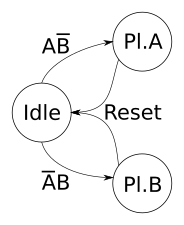 More formally, there are two players A and B with a button at their finger tips
of same name. The state transition diagram has a default state Idle
where the game starts and the buttons are assumed in the
A B
state. If player A presses, then transition A B is taken and
player A wins. If player B presses, then transition A B is taken and player B
wins.
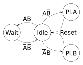
The game is reset by pressing the reset button. No other transitions are possible. If both player A and B press at exactly the same time (combination A B), nothing happens. There are a few corner cases. For example, what happens, after both buttons are pressed, while the system is in the idle state and one button is released? You'd expect to have an idle state where both buttons must be released before the game can start. As you can see, sometimes a simple game is not that simple. The state diagram on the right solves this problem by introducing a wait state, which is only left when both buttons are released again. This would be an good solution because all relevant button combination have a defined outcome. However, it is not entirely sure if and how this can be implemented. 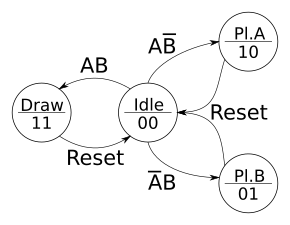
There is a small modification to the state diagram, which makes implementation easier. The situation where both players press at the same time may be considered a draw. That also means that it is alright to show this situation by having both LEDs turned on at that time and have this as a stable situation. The question open at this point is "is simultaneous press actually simultaneous?". Dealing with the real world does not always allow for perfection, but it is a question of how perfect it can become. How many ways are there to make such a circuit? Well, plenty, but there are advantages and drawbacks to each design. That is where it gets interesting. What are the advantages and drawbacks and what does that mean in practice? What do you need to check and test? This is where proper engineering excels; making informed choices and using compromise to achieve a goal. Some may say we are just making things more complicated by thinking too much, but engineering means to make well-informed choices and balance the advantages and drawbacks to achieve the design goal. Then again, if you make a mistake, take a look at this project and consider pressing one of its buttons. Lets look at three designs to achieve the goal set out: (jump to final result) Micro-controller based design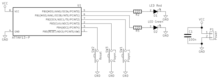 Reaction tester using micro-controller (schematic file as PDF)
Modern times have given us small, cheap and plenty of micro-controllers. You
get a whole lot of functionality in a small package and you just write some
code to add the intended functionality. Seems simple and fine... Until you look
in depth.
The advantages are almost entirely due to the reduction in components. Component count is a major factor in production cost, as each must be placed and soldered onto a carrier. However, the advantage is partly offset by the programming requirement, which introduces an additional step in production, but at the same time makes it more flexible. The second drawback is power consumption. If the reaction tester is running, then the MCU must be running, which has a non-zero power consumption. The design may in fact not function as intended and the results may be unreliable. This is due to bouncing of the switches and the time it takes to detect which button is pushed. If both players press rather close to each other, within the bouncing time of the switches, then the reverse situation may be detected. Solving this problem may proof to be very hard or, indeed, impossible. Please note that it is not a question of "works most of the time", but it must be guaranteed to work every time. Rule #1 in practical engineering: "Anything that can go wrong will go wrong". The MCU would run at 8MHz (internal RC oscillator). The detection of the buttons is somewhere at 8 clock cycles from real time (coded very tightly). That is one microsecond where you may get into problems. If the MCU is sleeping for power preservation, then the detection times will deteriorate even further into the millisecond range. At that stage, we are significantly in the "will not work" region of design. A real photo-finish is often under a millisecond. Mixed gate-type based design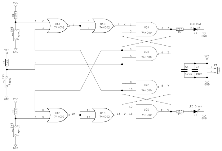 Reaction tester using NOR and NAND gates (schematic file as PDFe)
Back to basics, use good old gates and make a latched system. The basis
are two SR-flipflops to hold the state. Both latches can be reset to the idle
state and the player buttons flip one of the latches. Once a latch is flipped,
a lockout mechanism, using an OR gate (NOR + inverter) prevents the
other player from changing the state.
The behavior of the system can be simulated (used Qucs). The "draw" when pressing both button A and B is in the order of 14ns according to the simulation, which corresponds to two propagation delays of the gates (both NAND and NOR exhibit 7ns propagation delay). An initial 20ns reset is performed to get the system in a known state before activating the buttons A and B. Please note that the time-scale (dtime) is not linear, but strictly monotonous. 
Win A when |tB - tA| > 14ns (at 15ns in simulation)

Draw when |tB - tA| < 14ns (at 13ns in simulation)
The system is symmetrical, so a win for A and a win for B means that they just
need to be apart >14ns. A draw happens when B is activated before X (or A
activated before U). In other words, a draw happens while the lockout is not
yet in place. The bouncing of the buttons is of possible importance because
there is a minimal "on-time" required. However, when a pushbutton hits the
first bounce, then the chances are great that it will be in the microsecond
range, and thus be no problem. The on-time is simulated with just 50ns and that
is more than sufficient.The simulation predicts an oscillation at V and W when the time between A and B is exactly 14ns, where both V and W alternate simultaneously between high and low. This is an artifact that will generally not occur in practice due to the slight differences in the gates and wiring lengths. Very small timing differences in the paths (<1ps) have no oscillation. Therefore, it is highly unlkely to be of any concern. A second oscillation will (most likely) occur when you press both A, B and reset buttons at (almost) the same time. The button press detection is active-low, which means that the NOR gate will depend on the second input, which is the lockout feedback. This means that there is a loop in the system with high gain and there are only propagation delays in between. The loop is non-inverting, so when it oscillates, it may be stable or dampened. It depends on the timing of the buttons and the propagation delays what will happen. Once reset is released, a stable situation is reached.  
The circuit has the potential for bad behavior. Oscillation when all three buttons are pressed
Single gate-type based design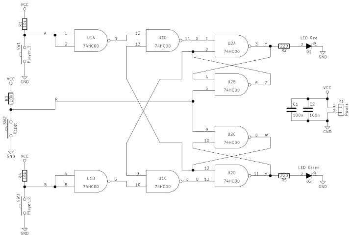 Reaction tester using only NAND gates (schematic file as PDF)
Doing some Boolean equivalence calculations quickly makes it clear that all gates may be of one type (either NOR or NAND). The basis are again the two SR-flipflops to hold the state. Both latches can be reset to the idle state and the player buttons flip one of the latches. Once a latch is flipped, a lockout mechanism, using a NAND gate, prevents the other player from changing the state. Changing the gates means changing polarity of the input, which is done by the left-over two NAND gates (there are 4 gates in one housing). This is not strictly necessary, but there is an advantage to keep the buttons in an active-low state (easier in PCB layout). The second polarity change is done by using the secondary side of the SR-latch, which has opposite polarity.
The design is now stable. The only oscillation that may occur is when buttons A and B are pressed at exactly twice the propagation delay of the NAND gate and everything is 100% symmetrical. The simulations cannot create an oscillation with even a 1ps skew. Therefore, the oscillating scenario is deemed extremely unlikely. 
Win A when |tB - tA| > 14ns (at 15ns in simulation)

Draw when |tB - tA| < 14ns (at 13ns in simulation)
The system is again symmetrical and behaves like the NOR variant. There
is functionally no difference. However, there is now only one type of
chip required, which is cheaper in volume than having different types.No oscillation will occur if you press both button A, B and reset. The reason is the change of polarities, where the lockout feedback was changed to the secondary gate of the SR-latch. The reset activation forces the SR-latch into a stable mode because the feedback is forced to follow the reset. 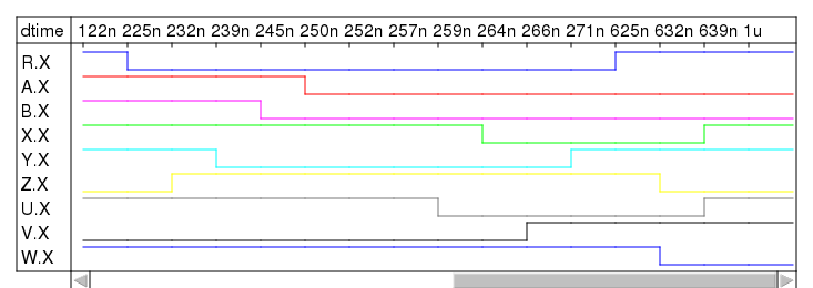
NAND version is stable when all buttons are pressed
It is interesting to see that the timing for win/draw is exactly the same for the NAND version. The reason lies in the change of polarity from the SR-latch feedback. Both input signals in the lockout mechanism needed to change polarity, which means that one delay through a (inverter) NOR gate got replaced by the secondary SR-latch NAND gate. Unfortunately, it is difficult to reduce the win/draw window of opportunity without considering the stability of the system. A two-gate delay would be fair for most circumstances. Better use faster chips. The 74LVC00A has a propagation delay of 2ns, which would make a 4ns window instead of the 14ns for HC chips. Final resultThe single gate-type NAND version was put onto a PCB and tested. It works like a charm. There were only 74AC00 chips available at the time, but they are just about the same as HC chips. You can get the design files, which are made with KiCad. The layout is kept as symmetrical as possible and the A/B buttons are next to the LEDs. Power is supplied using three AA batteries in a standard battery-holder and the PCB is stuck onto the battery-holder with double-sided sticky tape.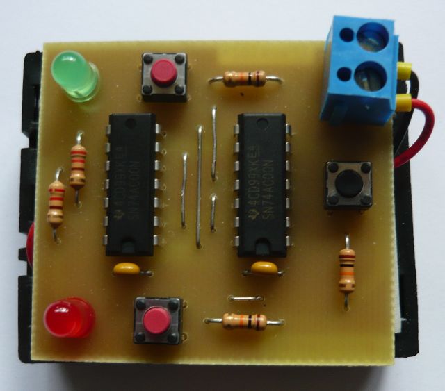 Final version in the real world (click image to enlarge)
The idle current is so low that I have not yet been able to measure it
correctly. I'm going to need a µV meter. I guess that the batteries will
last some time. Not once has it been possible to get a draw. Many hundred tries
so far, but no success. It is really hard to hit the buttons within 14ns of
each other (well, actually <12ns with the AC chips, but more complicated
because tPHL and tPLH are not the same).As for the initial question: "is simultaneous press actually simultaneous?": No it is not, there is a small chance for a draw. That result, however, means that a different design is required for some other specific practical use, where a draw must be impossible. If there may only be two active states, then the problem gets a bit harder because some sort of asymmetry must be designed into the system. That is something for another time and place.
Posted: 2016-06-28 |
| Overengineering @ request | Prutsen & Pielen since 1982 |