

 |
 |
|
|
RF74xxID
The Multifunction Passive 7400 RFID Tag
The new 7400 competition 2012 is on and something new has to be made. My honor is at stake after winning last year's competition (winkwink). I did have a few vague ideas to start with, but none of them was enough to get that wow feeling or you're insane impression. Some serious overengineering was required to match my previous capacitive scanner. At the local hackerspace OSAA I went on to start a brainstorm with pedersen, Asbjørn and Flemming, who promptly came up with a lot of funny ideas. All nice and well until Flemming mentioned RFID (he is the creator of the hackerspace's access system, HAL900, which is based on RFID). Now that is a thought. Of course, the first thoughts were with an RFID reader, but there have been made many of them already and that would be boring. However, the idea materialized to make an RFID Tag. I don't know who mentioned it first and, as with brainstorms, the ideas materialize as part of the joining of minds. The idea was born, make a tag based entirely on 7400 logic. 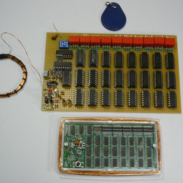 A tag's functioningAn RFID tag, sends a (unique) code modulated on a carrier wave. Most tags are passive, which means that there are no batteries and the tag only sends some ID data. Common tags use the EM4100 protocol. Many EM4100 compatible use the same internal transponder chip and are available in several configurations which differ in encoding protocol and baud rate. A general tag's transponder has the following features:
You can buy these tags everywhere like f.ex. Itead, Seeed or Sparkfun. The same places you can also get the RFID reader that goes with them. 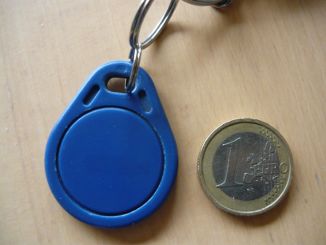 The design strategy follows rather easily from the specs and the general availability of the tags:
Getting powerThe main feature of a transponder is that it derives power from the EM field transmitted by the RFID reader. That would be a great feature to achieve, powering a 7400 based tag entirely on the EM field. A measurement was performed on the RFID readers that were available at the hackerspace using a simple setup. Take a coil, match it at resonant frequency with a parallel capacitor to 125kHz and see how much power can be drained.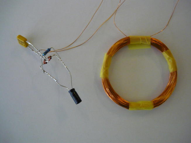 A bridge rectifier (with Schottky diodes) connected to the resonant tank (~3.3mH with 470pF), terminated with a 10µF capacitor, was drained by a resistor at 4k7, 12k and 47k. It turns out that the maximum power transfer occurs at a current load of about 700µA, where the voltage reaches about 19V (a simple quadratic interpolation of the measurement). With other words, more than 13mW of power can be drained from the EM field. The maximum current, while keeping the capacitor over 3.3V was about 2mA. This should be enough to power a lot of 74HCxx circuits. The 74xx family to use here is HC. These chips are entirely CMOS and have almost no static current draw (the quiescent current). They only dissipate on transitions of the inputs and outputs, which is specified in the datasheet as the power dissipation capacitance. Assuming 3.3V, 700µA and 125kHz, then the resonant tank can power chips with a total capacitance of 1700pF (U*C=I*t). This means there should be enough power to cope with a lot of chips and I/O pins. Using a higher frequency tag, like the 13.56MHz types, is much more problematic. The two orders of magnitude in frequency translate directly into two order of magnitude higher power consumption. And, since power is not a commodity in this design, it is pragmatically not possible to use the high frequency tags. A note on the HCT family: these chips cannot be used in this design. The HCT family has an average higher quiescent current and, more importantly, an additional current draw at each input due to the TTL level compatibility specification. The input stage of an HCT gate will source current when the input is not at the Vcc rail. This is specified in the datasheet as ΔIcc (additional quiescent current) per input pin. This current is at levels ranging from 10...1000µA, depending pin and load factor of that pin. This would mean that a lot of energy goes wasted and that is not what we want. Some analogue notes; the Q-factor of the resonant tank is an important factor. Higher Q-factor at same resonant frequency means less energy will be extracted. A small coil has fewer windings and will have less electromagnetic induction. However, a higher Q-factor makes it easier to modulate. The modulation is nothing else than changing the parallel resistance of the RLC circuit, which in effect changes the Q-factor: Q=R*sqrt(C/L). Both L, C and R need to be tuned for optimal performance withing the boundaries of operation. The balance needs to be determined by experiment. Tag designAn EM4100 tag features a data register, clock, power, modulation and control circuitry. Each part is implemented to be power conservative and create maximum flexibility.Schematic diagramIt should be noted that the final design includes all the bug fixes and some extensions that were learned from building a prototype; see PCB below for details of the changes. Here is the final design (to save you the trouble of falling for the TL;DR syndrome):Page 1, 64 bit shift register and parity calculation:
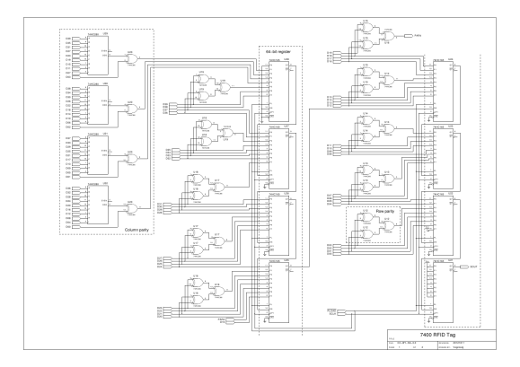 Page 2, power tank, clock, control logic, tag ID input and timing details:
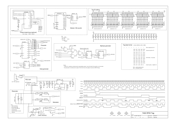 Circuit diagram as PDF. Circuit diagram gschem source. Data registerThe EM4100 tag has 64 bits of data, which means that the main feature of the design is a 64 bit shift register using eight 'HC165 8-bit shift registers. The register is reloaded every 64 shifts to reset the data and start anew. The data is input on the parallel input lines of the shift registers:
The row parity calculation (RPx) is done over 4 bits (each nibble). A parity calculation is an n-input XOR function and can be expressed by: RPx = D0⊕D1⊕D2⊕D3 = (D0⊕D1)⊕(D2⊕D3), which can be calculated with three 'HC86 XOR gates. The column parity can be calculated similarly using a 10 bit XOR chain calculation with an 'HC280 for the first 9 bits and one 'HC86 for the final bit. The good part of the tag's ID is that it is entirely static. For a design to be able to produce all IDs, it is only required to set the number statically with the switches and the parity calculation will not change. This has the great advantage that, even though it is using many chips for this circuitry (30/4 x 'HC86 for row parity and 4x 'HC280 + 1x 'HC86 for column parity), it will not draw any significant current. Hence, flexibility can be provided at no other expense than added chip count. Resonant power tankThe heart of the power supply is a resonant coil/capacitor setup. The signal is rectified with a low-drop bridge rectifier (from simple Schottky diodes) and put into a holding capacitor. The resonance of the circuit together with the Q-factor will ensure that a high enough voltage is generated. The input voltage is capped by a LED+zener. The LED will light up when the tank is full and will subsequently burn off all excess energy that enters the system, which protects the LDO voltage regulator from a too high input.The power tank holds enough energy to keep the tag going for some time. The LED+zerer limits the maximum voltage to about 12V and the LDO regulator needs under 0.4V to operate at 3.3V output. At a holding capacity of 2µF and an estimated maximum load of 800µA this results in (12V-3.7V)*2µF/800µA≈20ms. One full cylce of 64 bits of data at 2kbs is 32ms. The tank will at least be charged while the modulator is off (which is about 50% of the modulation pattern), so there should be more than enough energy. The setup is designed such that it is possible to have an optional battery supply connected too (3 or 4 x AAA in series will do) and the LDO regulator can be switched on/off with a switch. No battery should be needed, however, it is not guaranteed that all RFID readers supply enough energy and it is easy enough to add the option. The curious may ask themselves why the power supply delivers 3.3V whereas the HC family can operate at 2V. The reason is the PLL (see below at clock recovery). The VCO part of the 'HC4046 PLL will only work properly from 3V and up according to the datasheet. If the PLL is not used, then the whole power supply may be reduced to 2V. All HC chips are fast enough, even at 2V, to cope with the maximum frequency of 125kHz. Clock recoveryThe resonant tank swings at 125kHz and that is also the reference clock for the entire tag. A capacitively coupled bypass is created from the coil and entered into a 'HC14 Schmitt trigger to generate the clock RAWCLK (in the same way as you recover 50/60Hz clock signals from a mains transformer). The hysteresis of the Schmitt trigger is required because the entering signal has very slow transitions and will therefore pick up a lot of noise. A major problem is the induction of 50/60Hz noise in the coil, which translates directly into phase-noise on the recovered clock. The Schmitt trigger ensures high noise immunity and removes most of the 50/60Hz variability.An optional Phase-Locked-Loop (PLL), based on the 'HC4046 chip, synchronizes the carrier wave with the internal timing. The PLL is only required if the carrier wave exhibits discontinuities. Such discontinuities can arise from RFID readers that periodically throttle the EM field, which in turn can fall under the threshold of the 'HC14 hysteresis levels. However, the reader will often still be able to receive at low EM levels. The PLL keeps the internal clock running to bridge these periods. A switch is provided to enable/disable the use of the PLL. The PLL will also use a lot less energy when disabled, which in turn may be beneficial for operation with some RFID readers. Problems with the PLL may arise from cheap no-name RFID readers which may generate a carrier wave with a lot of jitter. This makes the PLL work hard to follow the carrier and increases power consumption. Another problem with the PLL can occur with really bad RFID readers where the recovery of the data is based solely on the RFID reader's internal 125kHz carrier. If the tag drops a period, then the reader may become confused and BadThings™ will happen (see cheap RFID reader below). Timing and baud rate scalingSeveral timing signals are derived from the master clock (MCLK). The EM4100 tags are apparently available in MCLK/16, MCLK/32 and MCLK/64 baud rates, although MCLK/64 (2kbs) seems to be the most prevalent. A selectable prescaler is created for setting the baud rate using half a 'HC393 counter, which results in DCLK. A series of switches select which divider will be used for the rest of the timing.The second half of the 'HC393 generates all internal clock signals (CCLK, PCLK and SCLK). The data register is shifted with SCLK, which represents the baud rate of the data stream. The complete timing sequence is provided in the diagram (page 2) to illustrate the operation. Counting to 128The data register is 64 bits long, but the problem is that the timing of the data-reload must be within one bit-period. If the counter only counted to 64, then the terminal count signal would be overlapping the shift-clock, which means missing one shift on the 64-bit cycle and results in a wrong start of the shift-cycle.A 'HC40103 is setup as a modulo 128 counter, counting down from 127 to 0 at double the baud rate and then reloads itself. The terminal count signal (MOD128) is then time-shifted slightly using CCLK to ensure non-overlapping flanks with the shift clock SCLK using a 'HC74 flip-flop to generate the parallel load signal PLOAD. Manchester encodingThe encoding scheme used by most tags is, as mentioned before, Manchester encoding. The major advantage of Manchester encoding is its simplicity to generate. The baud rate clock XOR the data stream equals Manchester encoding. A 'HC86 XOR gate combines the SCLK and SDELAY signals to form the encoded data stream.The actual data stream from the data register, SOUT, is delayed by one shift clock period to form SDELAY. When the data register is reloaded, then the SOUT signal is immediately changed from '0' to '1' (change from stop-bit to start-bit). However, the parallel load is not timed on the shift clock flanks as previously described and generation of the Manchester encoded signal must remain synchronous with SCLK so that no spurious transitions occur. The one SCLK delay makes all bits in the data stream synchronous with SCLK. The Manchester encoded signal is predicted to have glitches at the transition 0→1 and 1→0 of the data stream. These positions invert the SCLK signal, but the SDELAY and SOUT are not 100% synchronous. The glitch is caused by the SDELAY signal to trail the SCLK signal by the propagation delay of the 'HC74 flip-flop. However, the glitch is so short-lived (in the order of 10..30ns) that the modulator has no time to properly react to it, let alone the receiver, which has a huge amount of filtering. Therefore, the glitch is left as is. Biphase encodingThe second reasonable easy encoding scheme is biphase encoding (Biphase mark code or BMC for short). It is identical to differential Manchester encoding with a phase delay and is a FSK mode modulated with ASK. The difficulty of the biphase encoding is that the levels of the output are always alternating, whereas the frequency of the output changes with the data stream. This difficulty can be overcome by using a double-rate generator and then dividing the result by two.The first stage multiplexes PCLK and SCLK based on the data stream using a set of 'HC00 nand gates. The output of the multiplexed clocks is not glitch-free, for the same reasons above (SDELAY trails SCLK), but also because PCLK and SCLK are not synchronous. The 'HC393 is a ripple counter and that means trouble. A signal with glitches cannot be run through a divide-by-two setup without causing trouble (the glitches would be interpreted as clocks too). The multiplex output is cleaned of glitches by sampling the signal with CCLK, which is guaranteed to be active a lot later than the duration of the glitches, yet completely in sync with the master timing. Finally dividing the result by two with a 'HC74 flip-flip makes the signal complete. A set of switches can be used to select either the Manchester encoding or the biphase encoding. ModulatorFinally, the encoded signal has to be put back onto the coil to signal back to the RFID reader. Both ends of the coil are floating on both sides of the ground (it is an AC signal that is induced).Amplitude modulation on the coil is performed by creating a controlled ground short at both ends of the coil with a couple of MOSFETs, each taking care of a half period of the AC signal. The bridge-rectifier forms the closed path to ground for each side. Although the MOSFETs are able to react to the above mentioned glitches for the Manchester encoding, the resonant setup cannot as it is tuned 2..3 order of magnitude under the glitch frequency. Most images and diagrams you find on the net do not show this part or show it misleadingly incorrect. The short is both controlled, by means of the generated encoding, and limited to a very low level by means of resistors. A passive tag is normally very small and has order(s) of magnitude less power than this design. Tags generally have smaller coils and therefore can reach only very low modulation depths. If the big coil in this design is shorted completely, then it would, most likely, send a modulation signal so strong that it would confuse most RFID readers. Secondly, a shorted coil requires the use of the PLL because clock recovery would stop while the coil is completely shorted. Prototype buildingNow, if the theory and design are sound, then it should work like a dream. However, practice and theory are not always in accordance and my gray cells fail me too once in a while.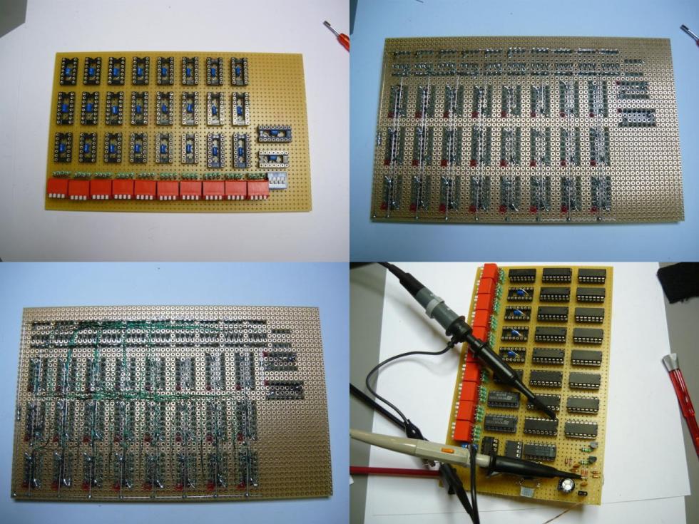 The prototype has 40 red DIP switches to set the tag's ID and 4 blue switches for the prescaler. The top row of 8 chips are the 74HC86 XOR gates for the row parity calculation. The middle row of chips are the 8 74HC165 shift registers to form the 64 bit register. The bottom left five chips are the column parity using 4 times 74HC280 and a 74HC86. The rest are the counters, PLL and Schmitt trigger. The soldering took about 6 hours in total. There are again a lot of connections. The prototype concentrated on proving the basic functionality and that it actually was possible to power the whole design from the EM field. The prototype only has the Manchester encoding implemented including the PLL setup. 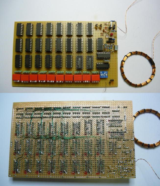
Debugging sessionsDesigning the basic tag circuit was not difficult. It took only a few hours to come up with the idea of the setup. However, some things were not planned carefully enough and some functionality had to be determined by experiment.The initial thought, taken from searching the net, was that the modulation was deep, very deep, and that the coil was completely shorted while modulating. That led me to spend a lot of time to make the PLL setup work properly and that is not always as easy as it sounds. PLL problemsThe problem with PLLs is that you need to balance several parameters to ensure stability within the operating environment. For one you need to ensure fast and stable phase locking while at the same time trying to reduce both the locking range and the drift with intermittent drive from the clock recovery. Using the datasheet of the 74HC4046 proved to be more challenging than expected. There are no fixed formulas for all components and some need to be traced from graphs (it still riddles me that there is a factor 2 discrepancy in the frequency from the component values from the graph tracing with respect to reality, oh well). It took some time to find suitable values for all components and ensure that the 125kHz was rather good in the middle of the VCO's range while at the same time the drift was reduced at non existing input drive.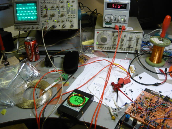 During drift analysis it was also discovered that a significant portion of 50Hz line induction drove the coil and effectively created a frequency modulation on the PLL's output. Holding a hand tightly on the coil removed this induction. The problem was that the PLL's input at the phase comparator showed threshold variability due to the non-binary behaviour of the input signal. The flanks of the capacitively coupled clock recovery are bad for logic circuits and it was determined that a Schmitt trigger would solve the problem. It is a notable property of the Schmitt trigger that its power consumption is very high at the transitions. A look at the datasheet shows an extreme rise in Icc in the transitional areas (see page 7, figure 9 and 10). The current consumption is high while the input is between the threshold levels. The reason for this is that the input stage is put into a linear operation mode in combination with a feedback from the output for hysteresis. Luckily, the time spent in the high power range is short and overall power consumption is limited. But still, the bare usage of a Schmitt trigger is a drain on the system. Cheap RFID readers and crappy signalsWhen I started the project, I had absolutely no idea how sensitive an RFID reader would be to the modulated signal. Modulation was therefore implemented as a full short of the coil, as found on the net. It soon showed that the modulation was way to deep and the RFID reader could not make heads or tails out of the signal. The internal reader electronics would simply be overwhelmed by the modulation and junk was produced.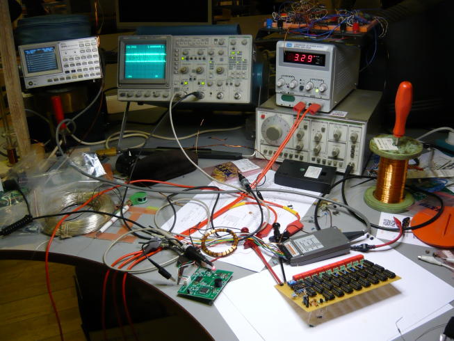 The lone RFID reader at the hackerspace had to lose its casing and a few wires were soldered on the PCB to measure what actual data was being received. It turns out that the RFID reader can receive the data with a coil short in the order of 50..100µA. This is somewhat far away from the 2.5mA which is generated with a full shorting of the coil. The added benefit is that the PLL is now optional. The clock recovery can be operational while the modulator acts on the coil. The residual coil induction will have enough drive to keep the clock detected. 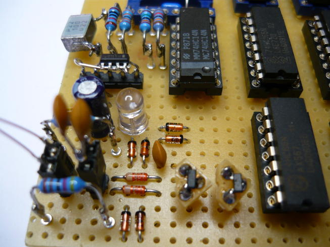 The modulator was originally designed using bipolar transistors. This caused the transitions of the receiver to be rather flat because the transistors were operating in a very low-power mode (and therefore somewhat slow). Changing them to MOSFETs made the modulator faster and saved another 27µA. I did only have some SOT-23 packaged ones and mounted them on a PCB with legs. The 3.3V LDO regulator at hand at the time, which was in SO-8, was mounted on a header with some wires. Read on for more modulator problems... The lone RFID reader is of no-name quality and makes all the promises you can expect. If you send junk data to the RFID reader, you will a) crash the RFID reader, b) send junk to the computer and c) curse hell and heaven together why things are not working as expected. All that to find out that you simply should have made your own RFID reader in the first place (it turned out that OSAA's own door system was much more robust and could cope with all I threw at it). Logic error debuggingAfter getting a decipherable signal at the RFID reader it still did not work as expected. Two errors popped up in the design.The first error was the modulo 128 counter, which was clocked at the rising edge of PCLK. However, it should have been clocked at the falling edge. The prototype was sending ten lead-in bits instead of nine because the generated PLOAD covered a rising edge of the shift clock. A simple inverter on PCLK solved the problem. The final design, with the biphase encoder, provides the PCLK signal as part of the encoder. The second error was the polarity of the Manchester encoded output. The only reference found on the net specified "low means high current" and a drawing showing a low-to-high transition for a logic '1' in the data stream. The description is fairly open to multiple interpretations. It turns out to mean: "low means modulator active (coil shorted)". Luckily, the delay of the data stream to form SDELAY results in both a positive and negative logic data stream. Simply changing the Manchester encoding to use SDELAY was trivial. Passive power testThe power consumption of the entire prototype was measured to see if a passive system would be feasible. The current draw at 3.3V was hovering at 780µA; low enough to close the loop and make the prototype passively powered.And then,... nothing happened with the cheap lone RFID reader. All was working as expected, power was available, data was being sent and then, suddenly, "BEEP". The code was read correctly and shown on the computer with the RFID reader. Success! The door can now be opened with a homebrew RFID Tag. 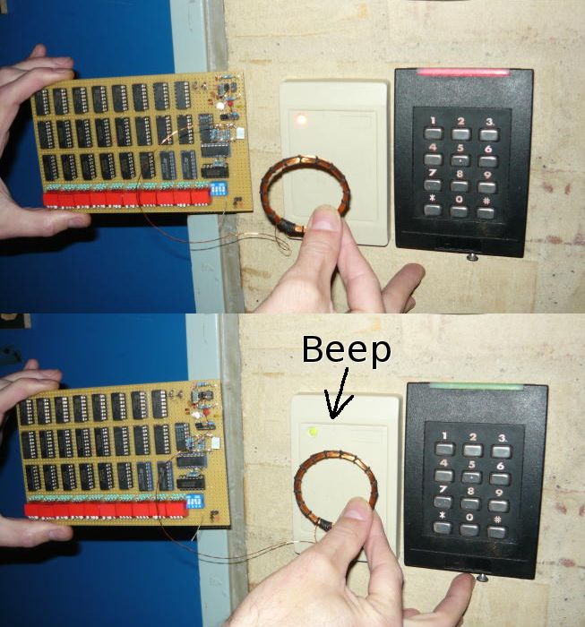
The quest for resonant powerThe power from the resonant tank needs to be tuned in such way that the RFID reader is not disturbed too much, while at the same time guarantee that enough energy is extracted to operate the tag. This turned out to be a greater challenge than expected. As mentioned before, the Q-factor plays an important role. You actually want a small coil, large enough to get energy, but small enough not to load the sender too much and modulate as easily as possible.Please note that the resonant tank's LC circuit (C100/L100) is not exactly resonant at the theoretical frequency of the components combined. The reason for the discrepancy is that the tank is (slightly capacitive) loaded by the tag. Therefore, the coil must be a bit smaller than what you would expect. This has the advantage that you can make a coil on specification and then remove windings until it swings correctly. It turned out that the lone cheap RFID reader was very sensitive to high loads and that lesser loads would make it work better. The initial coil, 3.3mH, was changed and halved in value several times until a somewhat stable compromise was found at about 680µH. The second change was to reduce the overall load capacitance from the holding capacitor from 10µF to 2µF. The lone RFID reader still crashes now and then, but at least it works more often than before. Anyway, OSAA's door controller still seems to be happy with anything I throw at it and it hasn't let me down once (even when I forgot my real key while testing). 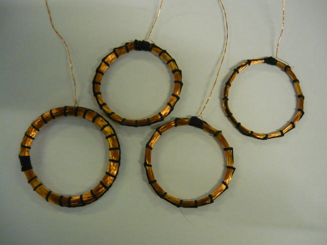 The no-name lone RFID reader works fine when the tag is powered externally. When using an external power source, the PLL needs to be enabled for best result, apparently. My best guess is that they saved too much on decoupling capacitors ;-). After a discussion at the hackerspace with Mark (the guy who uses this crap reader), he told me that he had seen trouble with the reader before on his computer, even with genuine tags. It seems that there is a bit more to it and a small crap-reader-debug-session was arranged. The power supply of the lone RFID reader showed 200mV ripple on the power supply (at 125kHz, from the resonant coil setup) and some nasty pulses here and there. Soldering an extra 1µF + 100nF capacitor on the board on a place that was marked on the silkscreen, but was unused, actually improved its performance considerably and now the lone RFID reader crashes even less and can get the prototype to be read with passive power enabled. Note to all: don't buy these junk-readers. Either get a good one or build one yourself. If you think that the story ends here, you are wrong. The modulator still has room for improvement and a significant operational change made it work much better. Even the no-name lone reader can be made to work better. A real PCBAfter looking a while at the original design, and pondering my options, it was decided that this gadget was simply too much fun to be left alone as a prototype. It simply begs for some more attention and completing the overengineering step to ridiculous proportion. A PCB was designed and, with some care, everything fit on a 50x100mm PCB in 2 layers without running into "No space left on device" errors. The 50x100 size means affordable bulk PCB from ITead or Seeed (yay!). However, making a credit-card sized PCB proved to be too much trouble.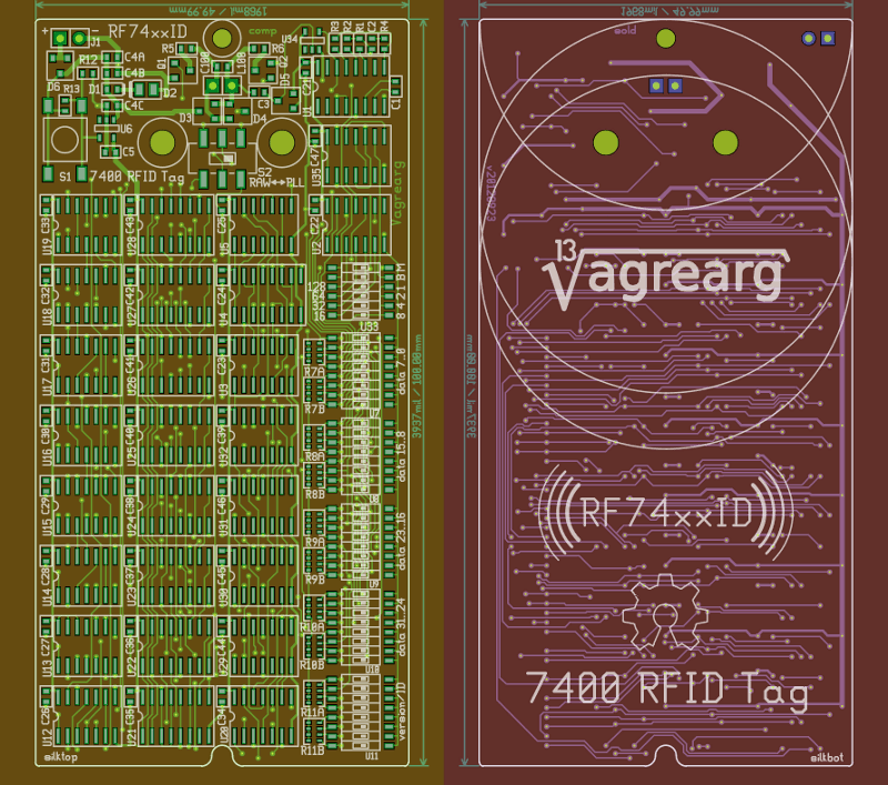 The PCB is designed with all SMD components to get it to fit. There are 412 vias with 0.3mm holes and traces/clearance in a 7mil design. All possible features are implemented with complete tag-ID control via DIP-switches, optional external battery or passively powered, switching between raw clocking and PLL clocking, both Manchester and biphase encoding and scalable baud rates between 1, 2, 4 and 8kbs. You can get the PCB design source and the gerbers used for production (please do not use these because of errors in the design). The files are not for production at ITead or Seeed, so please read the readme for details. China had the mid-autumn festival plus national holiday where all things get delayed. The production run had be to delivered well before 31st October to meet the contest deadline. I'm going on a limb here, but with the feedback from guys at the local hackerspace, I'd say there are at least three who want this device. Maybe just for fun or for other uses (like testing your SMD soldering skills). You can get your own RF74xxID tag too. Let me know if you want one. If there are many who want one, then I can make it a kit or produce them assembled. The prototype taught a few lessons which were incorporated into the final design and PCB version.
The BOMThe raw component cost is under $30 (excluding PCB and coil). The coil you will have to make yourself (see below). Actually, the DIP switches and the PCB are the most expensive components.You may change most components with your homebrew stock. However, the input capacitors should be able to withstand at least 16V. Secondly, you should use 1% resistors and 5% capacitors for the resonator and the PLL to ensure to be on the calculated target. It should be noted that the decoupling capacitors are all 10nF (instead of the usual 100nF). The reason for this is to reduce the load on the resonant power tank. The design is rather low frequency and it can tolerate slightly increased noise on the Vcc rail because it operates well above the minimum Vcc level. The coil is calculated to be 89 windings of 0.4mm SWG 26 wire with an average (center-line) diameter of 50mm. The coils made were wound on a core with 48mm diameter (on a silicone sealant cartridge) and subsequently laced with a waxed cord to get it to form a nice donut shape with nicely packed wires. The correct resonance point is probably reached with 88 or 87 windings, depending tolerances. You may make the coil any shape you like (like square or rectangular), as long as you get it to resonate properly. However, changing the shape will require some experimentation as the dimensions are important for the inductance and the achievable EM coupling (see below for rectangular coil). If you measure the inductance of the coil, be sure to measure/test it at 125kHz. The inductance is dependent on frequency due to parasitic capacitance of the wound wire and EM field coupling behaviour (for example the 3.3mH coil measures less than 100µH at 1kHz). The parasitics will also influence the resonance frequency and achievable Q-factor. Security noteAs you can see, it is trivial to emulate RFID tags. All places where you only have to present a valid key for access are vulnerable to a replay attack. RFID tags in access systems should only be used in a "something you have, something you know" scenario (although, it might be ineffective).Even tags with encryption are vulnerable to a multitude of attacks. It is also becoming easier to emulate tags with the implementation of NFC in smart-phones (usually operating at 13.56MHz). Just write an application to modulate the EM field correctly and you can do whatever you want. As a standard disclaimer, all responsibility for (ab-)use is disclaimed. You, the reader, are responsible for your own actions. The messenger is not the bad guy. A case tooSometimes you have a lot of luck. A nice case would be great now the prototype is finished and the PCBs are on order. Exactly timed right, Flemming got the OSAA PhotonSaw to work. After he had spent a year working on the project he got the laser to cut its first pieces. Flemming and Rune made the final adjustments and put the alu-casing of the laser cabinet in place over a long weekend. You can imagine that we all were very excited to see things work.With the PhotonSaw working (albeit slightly experimental) we were able to test the first designs in real life and a case for the RF74xxID was designed in 2mm PMMA. This case is the first real target object ever made by the PhotonSaw, Yes! 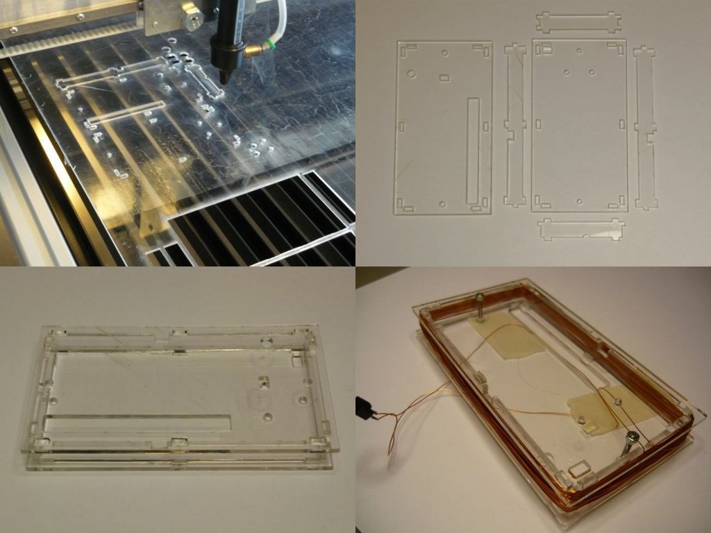 The idea was born to put the coil on the outside of the case. The first thought was to use half the case's height, but that didn't work out in practice (the extra holes in the long sides are therefore unused). But the coil fit just fine covering the entire contour of the case, even though I had some reservations whether the rectangular diameter (105mm x 55mm) would become too large to get a good EM field-coupling. A test-coil was wound, without any calculation, using SWG 26 wire and 66 windings. And, when you say you get lucky, you apparently have a lot of it because the coil ended up to be exactly right on target and measured around 645µH, which resulted in a resonance frequency of 125.2kHz with the tag connected as load. A test at the door showed that it worked just fine and the prototype works flawlessly with the coil. The height of the case can now be reduced with the coil on the outside of the case. The internal height is now only dependent on the components on the PCB and that should measure about 6mm including PCB thickness. Also, a bit of engraving would be nice. A suggestion from Flemming was to curve the outline a bit for both aesthetic and practical reasons (it slips better in your pocket). The curve will also protect the coil better, lying deeper, because it tends to extend outwards where no explicit pressure is on the wires. 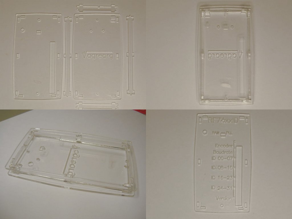 The PhotonSaw is not yet completely up to par. The engraving on the top was significantly misaligned and dropped. The "slightly experimental" state has to be fixed before a final case can be made. The curved contour also exposed a calculation error in the software where the beam did not return to the correct position while tracing a closed path. Anyway, the curves on the case make it look really slick. PCB assemblyThe real deal has arrived: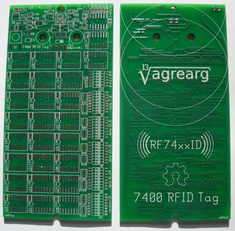 The assembly was not too hard. A stencil was used to put solderpaste on the board and then placing components was all that was left. Baked in the homebrew reflow oven and done. 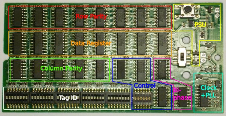 Testing the PCB version, however, proved to be another ballgame. Errors discovered in the (first version) of the PCB:
Energy feed-throughA lot of power could be saved with a new LDO regulator with shutdown facility (the MCP1804). The reasoning behind it was that a potentially connected battery could last longer if the tag could be switched off into a very low current mode. This change made Vcc floating while in the off-state. However, when the coil is located at the reader, then a feed-through is created by the clock recovery circuit.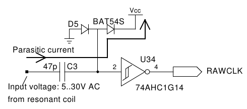 The capacitive coupling, C3, originally 47pF or ~27kΩ at 125kHz, feeds into the Vcc rail with the protection diodes attached. The energy pushed from the coil into the Vcc rail lets it reach about 1V. The current can reach 250..500µA on average. Surprisingly, the HC chips seemingly work at this Vcc level. Unfortunately, strange things also happen at this Vcc level. The 74HC(T)xx chips have an internal reset circuit (see HC(T) User Guide chapter 17) and it must be assured that it kicks in. Note that removing the protection diodes (D5) does not help. The HC's internal input protection diodes will kick in and do the same job. The power-on-reset is only triggered if Vcc drops below a certain value for a period of time. If Vcc is kept too high, then the internal logic can become confused because some parts may be in limbo while others work properly. An internal reset is required to set the chips into a consistent state. Therefore, Vcc must drop to a very low level for a functioning design. The symptoms observed were that the tag would function some of the time, and when it did, it would actually send the correct data all the time. When the coil was removed from the reader and placed back again all bets would be off. Sometimes it worked, sometimes it did not. Disabling the PLL made things worse. The lower power requirements caused the reader intermittently to receive data with the power-button in the off state. That you can call a power-conservative design. The solution is two-fold: 1) reduce the feed-through by reducing the clock-recovery capacitor to 15pF and 2) add a resistor between Vcc and GND of 22..100kΩ to drain residual energy to an acceptable low level. The second measure causes a higher power-drain while running and is not really required with the smaller capacitor. However, it is an option to mount and is better than limbo-chips. Voltage vs current modulationThe modulator circuit proved again to be a real pain. The modulation would completely disappear when the coil was placed at a certain distance of the reader. This would also happen when moving the coil towards or away from the reader.The reason for the problems were in the modulator setup. The MOSFETs short the coil with a series resistor to a certain level. However, if the current drain on the coil from the PSU tank is high, then the modulator's impedance is significantly higher than the PSU tank's impedance. This causes the modulation depth to be dependent on the PSU tank's impedance and that is not good. The behavior was amplified by the choice of zener diode (D2) to limit the input voltage to a lower level than the prototype. 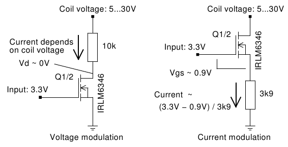 The solution was to convert the modulator into a current modulator instead of a voltage modulator. The series resistor for a voltage modulator is placed in the drain-to-coil path, whereas it is placed in the source-to-GND path for a current modulator. A resistor in the source-to-GND path will quench Vgs of the MOSFET until it is just over the threshold voltage (0.9..1.1V) and then operates the MOSFET in a linear region. A stable current will then flow independent of the drain voltage. A test on the prototype showed that a current modulator works very well. The lone no-name RFID reader would no longer crash (well, only once every 100 scans or so). It can be assumed that this change will work miracles on most readers and the tag will now probably work on most of them. Finished version #1You can see the patches made on the PCB. I had no 15p capacitor for the clock recovery, so it ended up with a through-hole patch for now. The modulator also has extra resistors mounted and wired at the source of the MOSFETs. All in all an acceptable compromise for the first version.All put together, it looks very nice, if I may say so myself ;-) (click quadrants for huge versions) 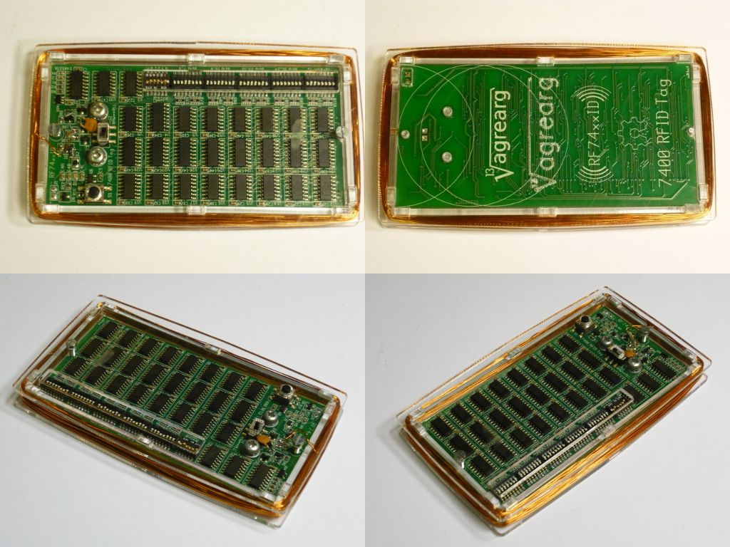 Your feedback is welcomed. It started out with three who wanted a copy, but while building this contraption already a few more asked for one too. If you want one, let me know. Video demoConclusionYou may think that, using 7400 logic, this project was retro-engineering, but you are partly mistaking. Firstly, The modern 74HC family of logic chips is not that old. Secondly, power conservative designs are always a challenge. Thirdly, the one-gate chips (as the Schmitt trigger used on the PCB) are rather recent developments. One often forgets that technology development does not cease on older chip families. It is just less visible and blends into the multitude of options available.The analogue parts were harder to design than the digital parts. Partly due to lack of specifications, but mostly due to the variability and multitude of compromises required to match parameters and unforeseen side-effects. Digital designs have relatively few options in design, whereas analogue parts mostly are a balance between different (and often orthogonal) design criteria. It shows that analogue skills of the engineers are an important asset in designing the digital world. I must admit that the 74HC chips are designed very, very well. The designers knew what they were doing to achieve such low power result. I had some doubt at the start whether the tag could be passively powered, but after reading through the datasheets and family specs it was just a matter of putting it together in the right way. Even though, there is still room for optimization in the tag's design part. Now lets see how this design will fare in the 7400 Contest 2012... Updates:
Posted: 2012-10-11 |
| Overengineering @ request | Prutsen & Pielen since 1982 |