

 |
 |
|
|
Decoupling by Example
Bypassing currents in overdrive
While enjoying the 7400 contest, it
occurred to me that many of the submitted logic designs lacked some of the most
elementary safeties to ensure a working result. One of the most disregarded
aspects of the designs was the lack of bypass capacitors. Then, with an
article
about Murphy's law linking a Maxim application note,
it was decided to write a bit about decoupling and bypass capacitors.As a person, who can be considered "old" in this line of work, I have experienced the problems of missing decoupling first hand. My first high-speed build was in the mid-eighties as an apprentice at a large electronics firm. The design I was building, a digital frequency measurement, used 74Fxx logic at a speed of 11MHz (which was very fast for the time). It was wire-wrapped on a double euro-card size board and used about 40 logic chips. When the time came to turn it on, I noticed that it didn't work as expected and all kinds of stuff happened all over the place. After checking the build several times I talked to my supervisor about the problem and he just looked at it and said: "There are no bypass capacitors; mount them on all chips over the power supply and we'll talk then.". Completely bewildered I did what he said and, as a miracle, everything just worked. Why would seemingly inert capacitance on the power supply make things work? My supervisor then told me all about switch/surge currents and inductance of the wiring and went on to tell the tale of decoupling. I admit that it took several years before I really understood what he was talking about, but the lesson was learned: always put capacitors on the power supply of logic chips. The terms "bypass capacitor" and "decoupling" are not some random words, but have a specific meaning in this context:
So why is this so important? Well, let me show you a picture:
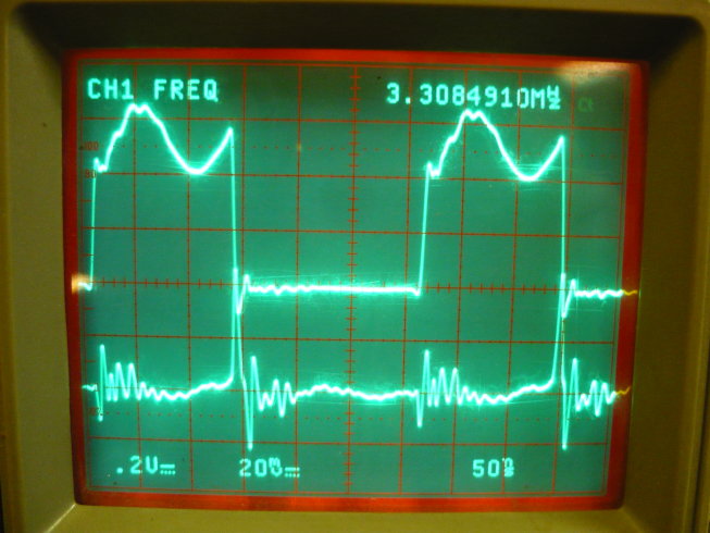 Figure 1: Missing bypass capacitor
Does this look anything like a digital signal? This is what you get without
bypass capacitors.Please note that the main operating frequency is irrelevant. The problem is in the falling and rising edges of the outputs. So, systems on a 1Hz, a 20kHz or a 50MHz clock require the same considerations. The used frequencies in the examples below are chosen such that visualization with the oscilloscope is easier. It should be noted that high frequency designs will fail faster because the number of transitions is significantly higher than in low frequency designs. However, this does not mean that low frequency designs are imune, far from it, they'll fail just as easily when Murphy is done. Oh, and btw, did you think about your little micro-controller running at 16MHz or the scanning LED controller to drive your light show? Measuring surge currentsTo see what is going on, one needs to measure the currents that flow. A simple test-circuit was created for illustration.
A pulse generator is connected to a 74HC04 inverter and the inverter is loaded with 10pF of capacitance. The output, TP1, is shown on the upper trace of the oscilloscope. The power supply on pins 14 and 7 is connected with a series resistor of 10Ω in the ground-path. The power supply current of the 74HC04 is measured on TP2 and visualized on the lower trace of the oscilloscope. The bypass capacitor can be (un-)mounted as indicated by the text. The oscilloscope probes used are 1:10 types, so all Y-values on the scope-image should be multiplied by a factor of 10. All unused inputs of the 74HC04 are grounded. The setup looks like: 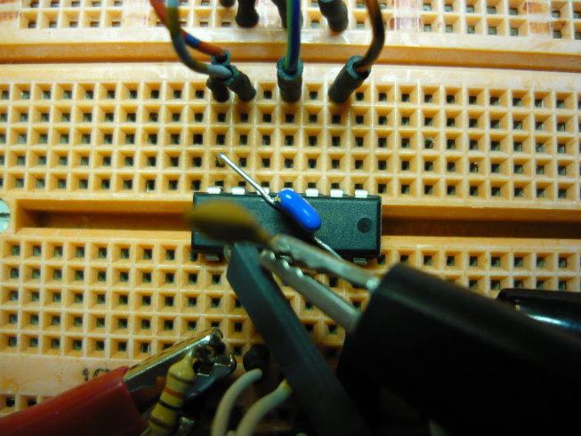 Figure 4: Breadboard setup
Figure 5 illustrates the problem at low and high input frequency. The left images are without and the right images are with the bypass capacitor mounted: 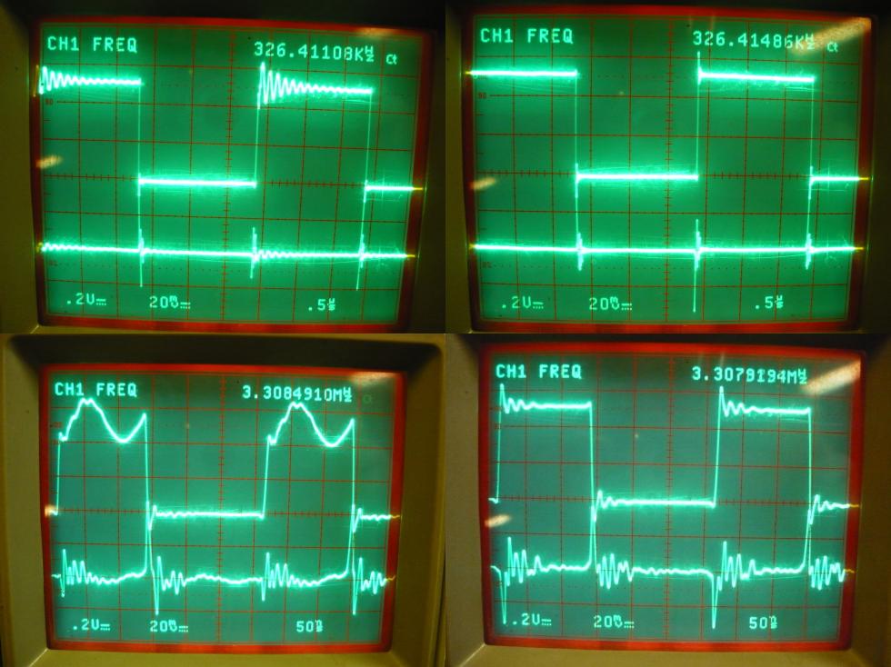 Figure 5: Output and current (left) without and (right) with bypass capacitor
Some observations from figure 5:
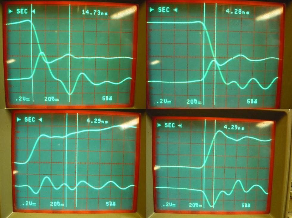 Figure 6: Edge detail of output and current (left) without and
(right) with bypass capacitor
The currents that flowThe 74HC04 is a complete CMOS design chip. This means that the static current draw is nearly zero. Current is drawn at high-to-low and low-to-high transitions. The transitions are where all load, parasitic and stray capacitance have to be (dis-)charged. The test-circuit from figure 2 has a load capacitance of 10pF. The pin- and stray-capacitance should be added to this, which would be something in the order of 5+2pF. The oscilloscope probe also has a capacitance, which adds another 10pF. The total load capacitance of the output is then about 27pF.Only considering this output capacitance, we are (dis-)charging the load in about 4.3ns to 5V. If a constant current is assumed (makes the calculation easier) we can estimate the current from above parameters using the charge equation: That means a huge current is flowing in and out of the output to swing it in either direction. Where does all this power come from? Well, from the power supply. It can be clearly seen in figure 6 that the current is not instantaneous, but builds up to a specific level and then falls off again. This behaviour clearly indicates an inductive element. This behaviour can be best seen in the right-two images of figure 6 (those with bypass capacitors), where the current (lower trace) peaks at the moment when the output (upper trace) is at zero. The current then drops, taking down the output with it. The calculated current compared to the measured ones line up quite nicely, considering that the calculation is a simple estimate. So why that bypass capacitor?Take another close look at the two lower images of figure 6. The left does not reach the 5V output level for some time, whereas the right one does so with no problem at all. There is not enough power available without the bypass capacitor to support the rising edge and it stalls at 4V for some time. Adding the bypass capacitor supplies the 74HC04 with instantaneous power for the duration.The bypass capacitor is about 4000 times as large as the load capacitance, which means that the expected voltage drop will be some 4000 times lower (in the order of 1..2mV) to support the transition. When the transition is the other way around, such as in the top two images of figure 6, then the bypass capacitor acts as a reservoir to accept the released energy. The load capacitance must be discharged and that current wants to flow to ground. However, the energy cannot move to the main power supply easily, but the bypass capacitor can store it temporarily. Power supply without powerThe main power supply cannot provide the logic chip with enough power because of inductance. Each and every wire exhibits (parasitic) inductance and causes current changes to be difficult. The standard equation in electronics for inductance: From this equation, it can be seen that change in current is inversely proportional to (the inductance). In other words, when inductance gets higher, it becomes more difficult to change the current in a given time-period if all other parameters stay the same. Additionally, a change in current means that there is a voltage drop over the inductance. A longer wire (or PCB trace) has higher inductance, and therefore works against fast changes in current and will exhibit a large voltage drop.The bypass capacitor is a local power storage. The bypass capacitor must always be mounted close to the chip's power leads, thereby reducing inductance from the bypass capacitor to the chip to a minimum. This setup decouples the main power supply from the chip's power supply. Stress on the inverterThere are 6 inverters in a package, so the test-circuit was changed to feed more current: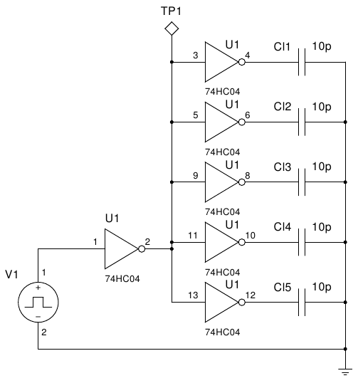 Figure 7: Additional load test circuit
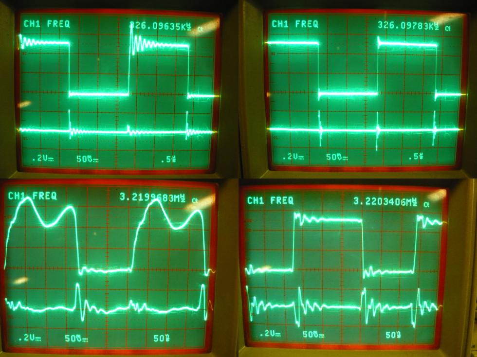 Figure 8: High load output and current (left) without and
(right) with bypass capacitor; note the changed current scale
The current at the GND pin now peaks at about 70mA when no bypass capacitor is
installed. A symmetrical image is again visible With the bypass capacitor
installed showing +/-50mA, depending falling or rising edge.Note that the transitions, as seen in the lower left image of figure 8, are significantly more flat. The 74HC04 simply lacks the energy to support the transition. Adding the bypass capacitor (image on the right) restores the transitions again to an acceptable level. 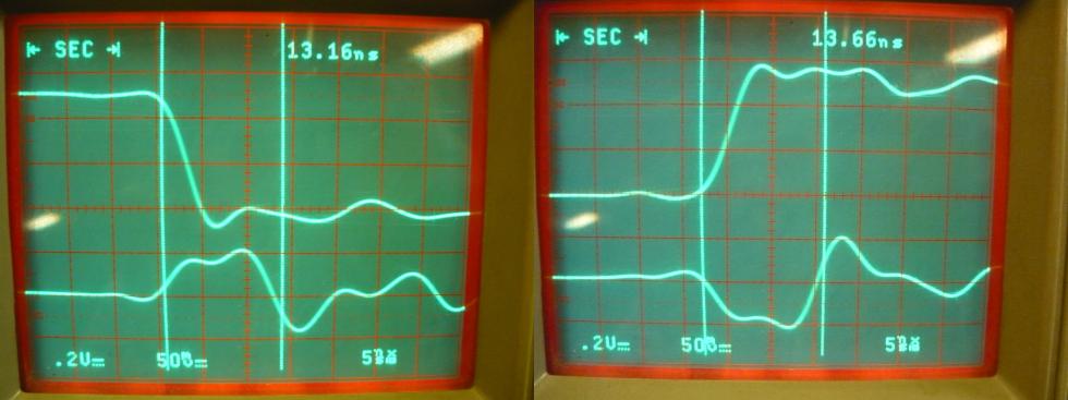 Figure 9: Edge detail at high load with
bypass capacitor; note the changed current scale
The details of the edges reveal an elongated current draw, which is caused by
the much higher energy demands. The load on the chip is about six times higher
(the first inverter is loaded with 5 times ~5pF of the secondary inverters'
input capacitance).This is just a simple example with a simple inverter chip. Now extrapolate to complex logic chips which have many internal gates with many internal transitions. There are many parasitic internal gate capacitances that must be (dis-)charged every time an input changes. Or, think about that micro-controller with many thousands of gates. GroundingFrom above explanation and visualisations it should be apparent that the bypass capacitor is an important element with a function. It stores energy locally and supplies it when necessary and receives excess energy.The local supply is always replenished from the main power supply via the Vcc connection. However, the excess energy has to be dumped into the main power supply over the ground (GND) connection. Dumping energy in the bypass capacitor raises its voltage, and, effectively, creates a temporary localized island at a different potential. Removing this imbalance is very important and is done through the grounding connection. PCB designs often have grounding planes which are very effective connections to the main power supply. A good grounding design is paramount to effective dumping of excess energy. But beware, a simple grounding plane may also introduce eddy-currents and multiple GND connections may introduce ground-loops. It is always a good idea to ask your friendly veteran designer neighbor. Most of the mistakes have been made and there should be no need to repeat them ad infinitum. Update: This article has apparently struck a nerve. It has been mentioned several places, including a translation into Portugese.
Posted: 2011-10-25 |
| Overengineering @ request | Prutsen & Pielen since 1982 |