

 |
 |
|
|
Lights Out, Turing Style
Building the device
Moving my behind to the local makerspace, OSAA,
to make this. It is going to take time and I plan to spend many hours there.
Luckily, there is coffee on the shelf and lots of sodas in the fridge (and
paying members have a key for 24/7 access).
The plan:
The schematic diagram was put into the PCB designer to optimize chip
placement. The rats-lines were minimized to reduce the wiring and see how much
there would fit on a board. The design is split into a logic board with all the
calculation stuff and a button/lights board with LEDs mounted on top of
buttons.
There are a little over 1000 soldering joints on the boards combined. Most
of them need to be touched twice (once to solder the pad and a second time to
add a wire). This takes a long time to make, estimated 15 hours of soldering
for the whole lot. The pictures below, of the logic board backside, were taken
with approximate one hour interval.
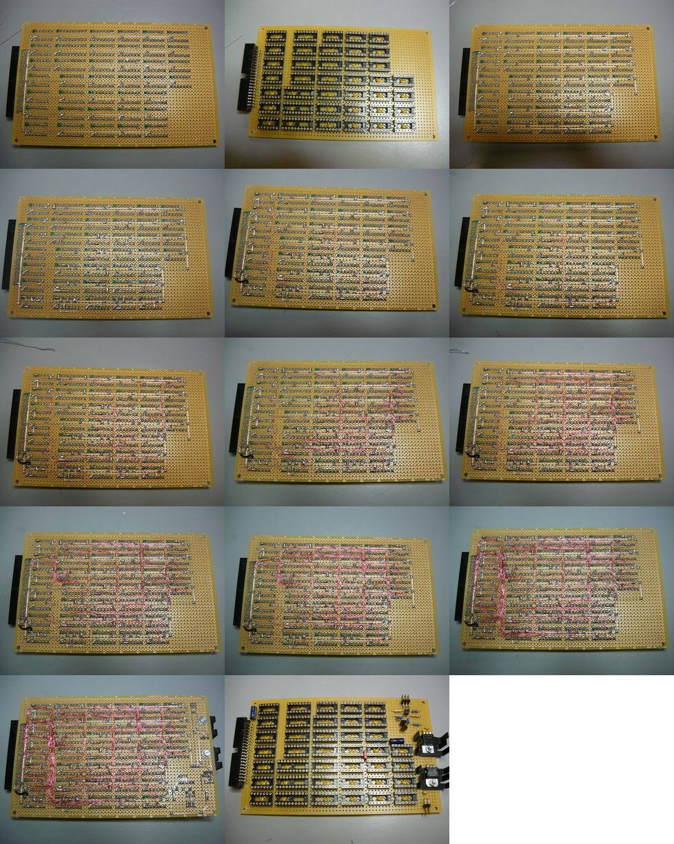 Illuminated buttons are a very expensive hobby and not in the budget for
this device. When asking for alternatives at the makerspace's mailing list, a
hackaday response, LED push buttons,
was the result. This was interesting, but I did not want to use two push
buttons for each LED as that would have resulted in 56 push buttons. The setup
was changed a bit to put the LED on top of the button. All LEDs are held by the
case's top plate (4mm acrylate), so centering the LED on the button and glueing
it in place should be enough. This is a € 0.20 solution that seems to
work well instead of a € 2.00 illuminated push button. Besides, now a
super-bright LED could be used and no extra buffers were needed.
Bending the leads in place and soldering the series resistor should hold fine. The series resistor was split in two because of symmetry (otherwise a wire needed to be added anyway; the leads of the LED are not long enough). The below picture shows a blob of hot-glue on the bottom (second LED in bottom row), but that step was later dropped because it was not as effective as anticipated. Actually, it was very hard to to keep the glue on the LED when pressed down on a (cold metal) plate. The glue would still stick to the plate and come off the LED too easily. Instead, the finished assembly was simply to leave the push button as is. Glueing the LED to the button had the drawback that it was nearly impossible to position the LED exactly over the button to fit the holes. So in the end used lower tech, but more effective. Making buttons with LEDs on top requires a lot of bending (where is
Bender when
you need him?):
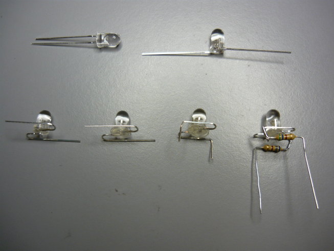 Some small changes in the layout were expected. The buttons for
controlling extra functions have been shuffled and the pot-meter got moved to
the top.
The logic board got a last-second change, where the 10n capacitor for the master-clock had to be rotated, to along-side, because the chips would not fit with the capacitor at the head-end (missing 0.5mm of space). The biggest change on the logic board was to add an extra voltage regulator (and adding an extra chip; see below). The only suitable wall-plug-PSU found on the shelf outputs DC 25V p-p unregulated. So a 15V regulator reduces the input and the input plug (which will be placed in the case) will be mounted with a 220..470uF capacitor. The switch-board only took 3 hours to make. Bending LEDs and adding the
resistors took 2 hours. And, the acrylate top had to be made too, with holes at
the correct position, which also took 1.5 hours of work:
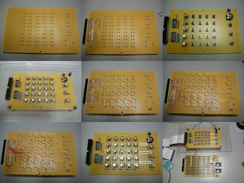 And ready for a first test with power on:
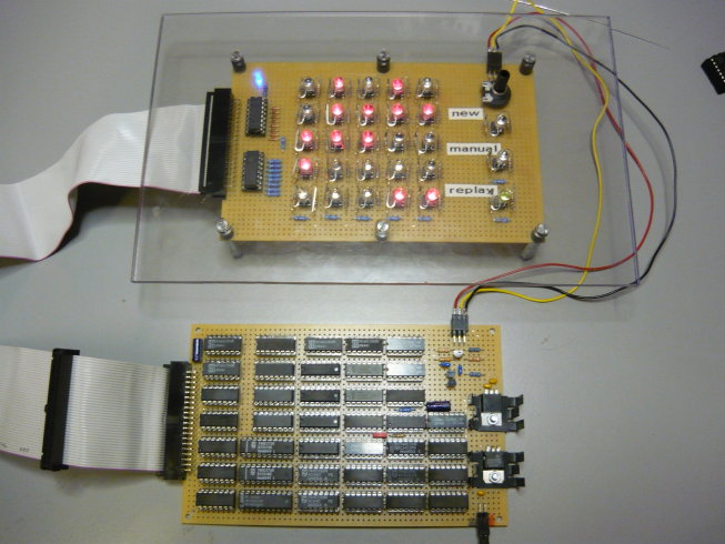 Finally finished building, now to start debugging. Of course there are
problems; the design is complex enough to have overlooked little things with
big consequences. So far managed to detect and fix:
All "defects" were detected during a hardware debugging session with a
logic analyser. The logic analyzer was donated to the makerspace, but nobody had yet managed to get it
working (it was tagged with a "hack"-label). Luckily, nobody dismantled it and
it is a very useful instrument when you know how to operate it
(the manual was in the box; wink-wink).
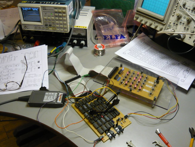 It works! The game-play is now working. Both manual- and game-mode
function as expected and a game can be played. The "solvable" indicator works
as expected and lights green when a game can be played (useful in manual mode).
And then a second debugging session to fix the last hitches:
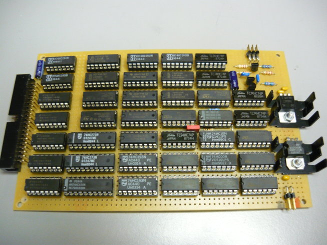
That completes debugging and the complete and fully functional board, as
seen below, includes the extra '74 chip at top right (there are 40 logic chips
on the logic board and 2 on the switch board):
 The final assembly has both the logic- and switch-board on top of each
other like a sandwich. They are mounted beneath the acrylate plate. Now a box
has to be finished.
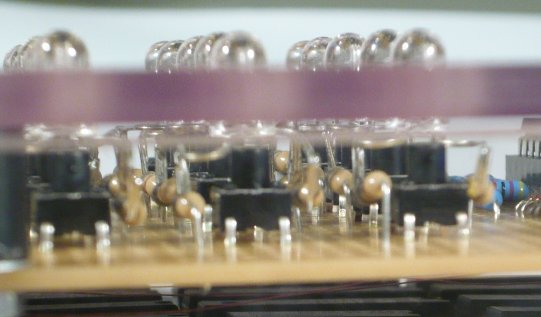
 Detail view of the LEDs on top of the switches through the top plate:
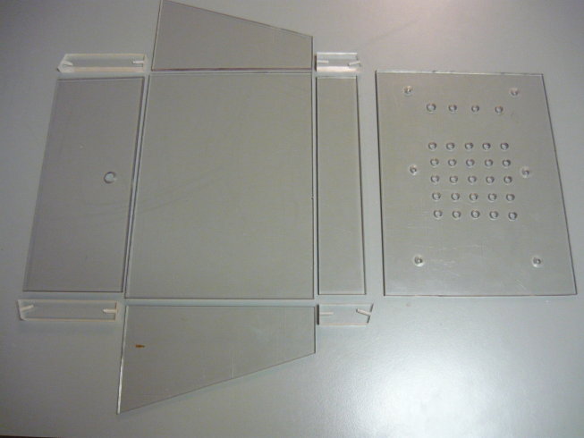
 The box parts:
 And finished!
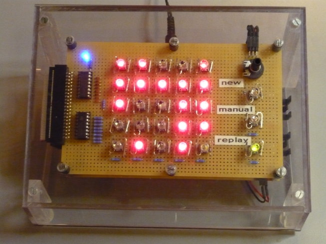 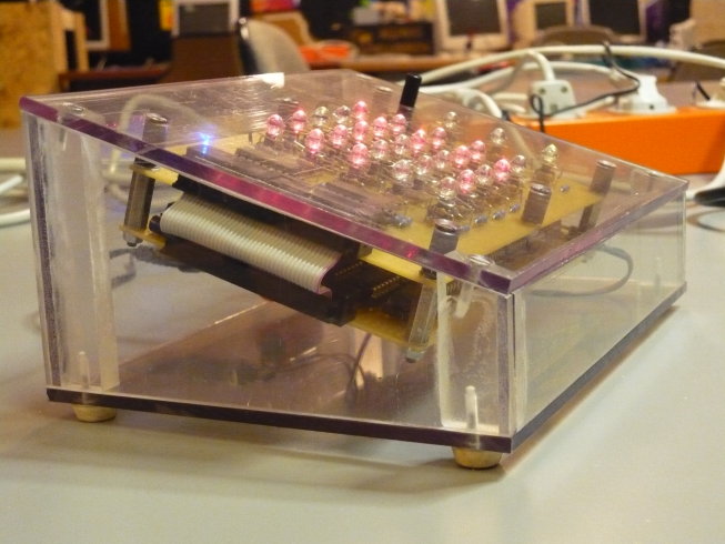 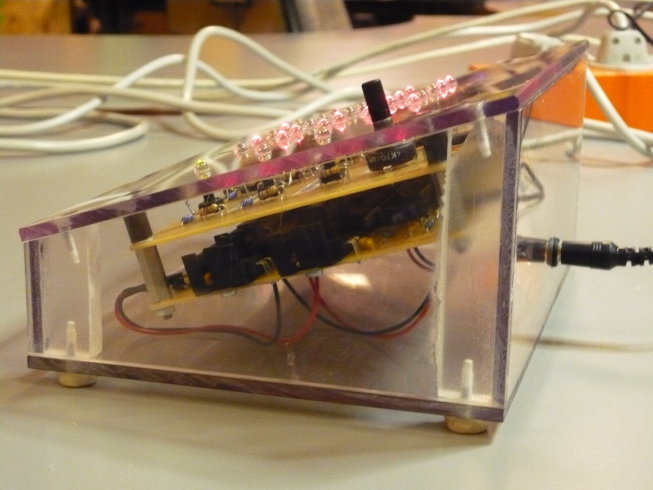 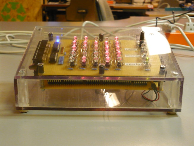 And there is a video:
Project entered into 7400 Contest.
Posted: 2011-09-25 |
| Overengineering @ request | Prutsen & Pielen since 1982 |